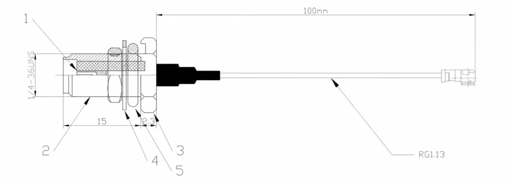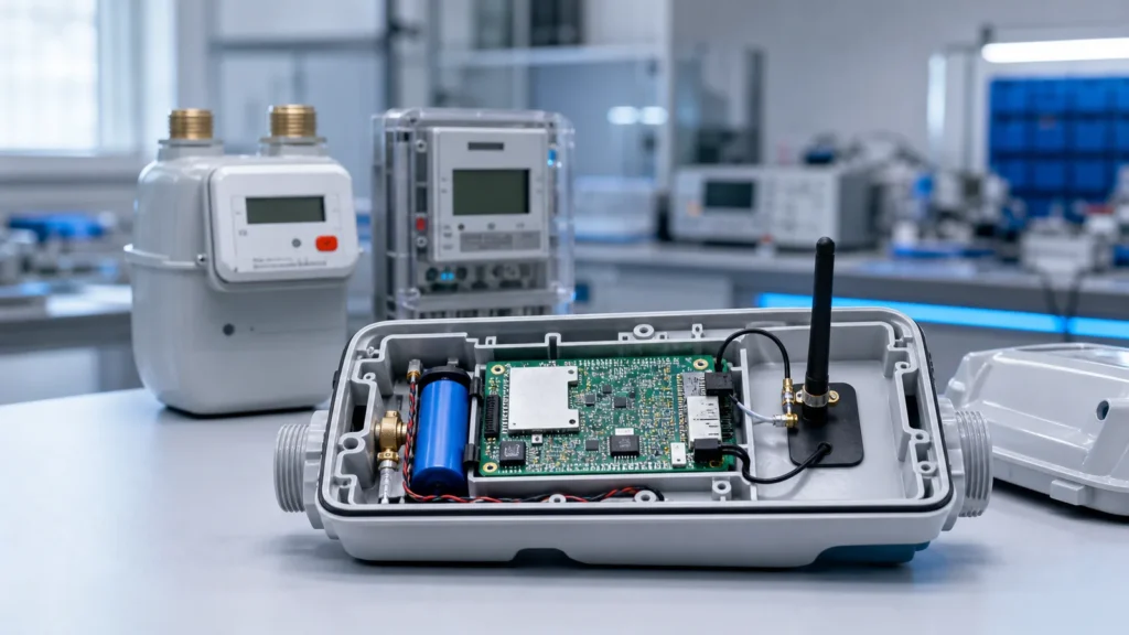

A PCB antenna is a radiating copper trace etched into a printed circuit board, which means the feed, the trace shape, the ground plane, the laminate and even the plastic housing all behave as one antenna system.
Short answer: use a PCB trace antenna when you have board-edge space, a ground plane at least a quarter-wavelength long at your lowest band, a stable enclosure, and volume high enough to repay the tuning work. Move to a ceramic chip antenna when board area is the hard limit, to an FPC antenna when the housing offers a better position than the main board, and to an external antenna when range, shielding or field replacement decides the product.
Here “PCB antenna” means a trace on a rigid board. A flexible printed circuit (FPC) antenna is a separate radiator joined by cable or contact — the same printed-conductor idea, a very different mechanical and RF problem.
The rest of this guide works through the four judgements that actually decide the choice: the bands you must cover, the ground plane you can afford, how far the enclosure will move the tuning, and how much retuning your schedule can absorb.
How a PCB trace antenna works
RF current runs from the feed into the shaped trace. The geometry sets the electrical path, while the ground region and nearby conductors decide how current returns, what impedance the radio sees, and how the field leaves the board. At resonance, part of the applied power radiates instead of reflecting back.

The quarter-wave rule, and why the vacuum number is wrong
Most printed radiators are quarter-wave (λ/4) structures: a monopole-style trace plus the ground plane forms the other half. In free space, λ/4 in millimetres is roughly 75,000 divided by the frequency in MHz, so a 2,450 MHz radiator lands near 31 mm.
That is only a starting point. A microstrip trace sits between air and laminate, so the wave travels through an effective permittivity (εeff) somewhere between the two. The physical trace ends up shorter than the free-space number by about 1/√εeff — which is exactly why the same DXF file cut into a different stack-up resonates at a different frequency.
This matters more than most layout guides admit. Standard FR-4 is not a controlled RF material; its dielectric constant is commonly quoted anywhere from 3.8 to 4.8 depending on glass weave, resin content and thickness. Because resonant length scales with 1/√εeff, a 5% swing in εeff shifts resonance by roughly 2.5% — about 60 MHz at 2.44 GHz, which is most of the 83.5 MHz available in the 2.4 GHz band. Treat that as an engineering estimate from the formula rather than a measured result, and it still explains why an antenna that passed on one laminate lot fails on the next.
The practical conclusion: the drawing does not determine performance. Board thickness, laminate, copper geometry, solder mask, the feed transition, matching parts and the enclosure all move the answer. A layout copied onto another stack-up, or placed beside a different battery, needs retuning.
Common PCB antenna layouts

Printed monopole and meandered trace
A printed monopole uses a board-edge radiator referenced to the PCB ground. Meandering lengthens the current path inside a smaller outline, but compactness can reduce bandwidth and efficiency. The exact trade depends on the full design.
Inverted-F antenna
An inverted-F antenna adds a shorting path near the feed. It is common in compact wireless devices because its geometry provides useful matching and size control. The feed-to-short spacing, radiator length, ground plane and keep-out region all matter.
Loop, slot and other printed structures
Loops, slots and planar patches solve different polarization, pattern and packaging tasks. They should not be treated as interchangeable trace shapes. Choose the topology from the band, board, ground reference and coverage need before optimizing dimensions.
What controls PCB antenna performance?
The bands — and the rules attached to them
The bands set the electrical size and the matching window. One narrow band is a different job from a cellular design covering several separated ranges. The bands also drag in regulation, because a printed antenna is part of the radio being certified.
| Market / rule | What it fixes for your antenna | Bands named in the rule |
|---|---|---|
| US — FCC 47 CFR §15.247 | Unlicensed digitally modulated and frequency-hopping operation, with limits verified as radiated emissions | 902–928 MHz, 2400–2483.5 MHz, 5725–5850 MHz |
| EU — ETSI EN 300 328 V2.2.2 | Harmonised standard for wideband data equipment under the Radio Equipment Directive | 2400–2483.5 MHz |
| Cellular devices — 3GPP TS 38.161 | Total radiated power and sensitivity (TRP / TRS) requirements for FR1 user equipment | FR1 operating bands |
Two consequences follow. First, your bandwidth budget is fixed for you: the 2.4 GHz band is only 83.5 MHz wide in both FCC §15.247 and ETSI EN 300 328, so a narrow printed radiator that drifts 60 MHz has already spent most of its margin. Second, cellular products are judged on radiated numbers rather than on what the chip delivers into 50 Ω, so antenna efficiency shows up directly in the 3GPP TRP and TRS requirements the finished device must pass.
PCB stack-up and materials
Trace width and effective electrical length follow from dielectric thickness and permittivity, so the laminate is a design input, not a purchasing detail.
- FR-4 is a family, not a specification. IPC-4101 slash sheets state dielectric constant and loss tangent at defined test frequencies such as 1 MHz, 1 GHz and 10 GHz, and different sheets carry different limits. Ordering “FR-4” alone does not pin down the number your antenna depends on.
- Loss climbs with frequency. Published laminate measurements put the dissipation factor of FR-4 epoxy materials in the 0.014–0.022 range between 4 GHz and 16 GHz. That is why sub-6 GHz designs tolerate FR-4 and higher-frequency work usually does not.
- Name the material on the drawing. When the antenna is small relative to wavelength, specify the laminate and thickness on the fabrication drawing and keep the same one from prototype through production.
Ground plane and keep-out
The ground plane is not a bystander. On monopole-style printed antennas it radiates as much as the trace, so changing its size, shape or stitching changes resonance and pattern. The keep-out region — cleared on every layer, not just the top — protects the current and field distribution from copper, components and cables that would detune the antenna.

Ground plane length is where compact products fail, because the requirement scales with the lowest band rather than with the size of your product. Using the same λ/4 ≈ 75,000 / f (MHz) relation:
| Lowest band | Free-space λ/4 | What that means on a small board |
|---|---|---|
| 433 MHz | ≈ 173 mm | Rarely available; expect efficiency loss or an off-board radiator |
| 698 MHz (cellular low band) | ≈ 107 mm | Longer than most IoT boards, and a common cause of weak uplink |
| 868 / 915 MHz | ≈ 86 / 82 mm | Needs a deliberate ground plane, not leftover copper |
| 2450 MHz | ≈ 31 mm | Achievable on most boards |
| 5800 MHz | ≈ 13 mm | Rarely the constraint |
These are geometric reference figures, not performance guarantees. Use them as a screening test: if the board cannot host the ground plane your lowest band wants, the fix is a different architecture or a different position in the housing, not a better trace drawing.
Feed and matching network
The feed transition must maintain the intended impedance. A matching network can correct a measured mismatch within limits; it cannot turn a poor radiation structure or blocked placement into an efficient antenna.
Enclosure and nearby parts
Plastic, glass, batteries, displays, shields, wiring and the user’s body can shift tuning or absorb energy. Final tuning belongs in the assembled product, not only on an open evaluation board.
Why a few dB of gain rarely buys much range
Datasheet gain invites a bad assumption: that a “better” antenna transforms coverage. The link budget says otherwise. Free-space loss follows the ITU-R P.525 relation, which in practical units is:
FSPL (dB) = 32.44 + 20·log10(f in MHz) + 20·log10(d in km)
Because distance sits inside a 20·log term, it takes 6 dB to double the range in line of sight. So:
- +2 dB of antenna gain buys about 26% more distance, not double.
- Losing 3 dB to a detuned antenna or a metal housing costs roughly 30% of your distance.
- A short coax pigtail with 1 dB of loss quietly takes back about 11% of range.
Run the arithmetic before redesigning: 3 dB recovered by moving the antenna away from a shield is usually cheaper than 3 dB chased through a new radiator. One detail is worth knowing here — the frequency term above comes from the shrinking capture area of a fixed-directivity receiving antenna, not from anything happening in space, as the standard free-space path loss derivation shows. On a small board, a compact and efficient 2.4 GHz antenna can therefore beat a compact but badly compromised sub-1 GHz one, even though the lower band looks better on paper.
PCB trace vs ceramic chip vs FPC
| Architecture | What it is | Main packaging advantage | Main development burden |
|---|---|---|---|
| PCB trace | Radiator etched into the rigid board copper | No separate antenna element; geometry can follow the board edge | Consumes board/keep-out area and depends strongly on the final board and enclosure |
| Ceramic chip | Discrete high-dielectric antenna component mounted on the PCB | Small, repeatable component outline | Still needs the specified ground, keep-out, feed, matching and final-device tuning |
| FPC antenna | Separate flexible printed radiator, usually connected by short coax | Can be placed on a housing surface away from the main PCB | Adds cable, connector and assembly placement requirements |
For an FPC example, GLFPC01 publishes 698–960 and 1710–2700 MHz coverage, vertical polarization, a U.FL connector and a 70 × 20 × 2.5 mm form. That product illustrates an FPC architecture; it is not a rigid-board trace design.
The ceramic antenna versus PCB trace versus FPC guide covers the three-way selection in more detail.
A practical PCB antenna development path
- Freeze the radio bands, conducted power, receiver targets and regulatory market.
- Reserve the board edge, ground region and keep-out before the mechanical layout is fixed.
- Check the ground plane against λ/4 at your lowest band. If it does not fit, change architecture now, not later.
- Select a topology that suits the available volume and the direction you need coverage.
- Simulate, or start from a reference design matched to your real stack-up and named laminate.
- Build tuning pads and measurement access into the prototype.
- Measure in the final enclosure with production-intent components, not on an open evaluation board.
- Tune, repeat across several samples and laminate lots, then verify radiated performance before certification.
Certification is not a one-time gate. Because a printed radiator is permanently part of the board, edits to the trace, ground plane or stack-up change the radiated emissions that were tested — so a late “small” layout change can send you back for retesting. Lock the antenna area before layout freeze.
When should you choose another architecture?
Choose a chip antenna when board area is scarce but the design can follow the component maker’s layout and tuning guidance. Choose an FPC when the main PCB is noisy or poorly located and the enclosure offers a better antenna position. Choose an external antenna when the product needs separation from shielding, greater installation freedom or a field-replaceable RF path.
If the antenna area, ground plane or enclosure is still changing, do not freeze the antenna. Those changes can invalidate earlier tuning work.
Share your band, PCB and enclosure constraints
Prepared by the Rftech Technical Team using current embedded-antenna references, published regulatory and materials sources (FCC 47 CFR §15.247, ETSI EN 300 328, ITU-R P.525, 3GPP TS 38.161, IPC-4101) and verified Global RF Tech product data. Sources checked August 25, 2026. Wavelength and link-budget figures are formula-based engineering estimates; validate the antenna in the finished device.
Ask our AI antenna assistant. Enter a keyword or question for a free answer based on this article, Global RF Tech content, and general antenna/RF knowledge.
Do not submit confidential or personal information. Privacy Policy