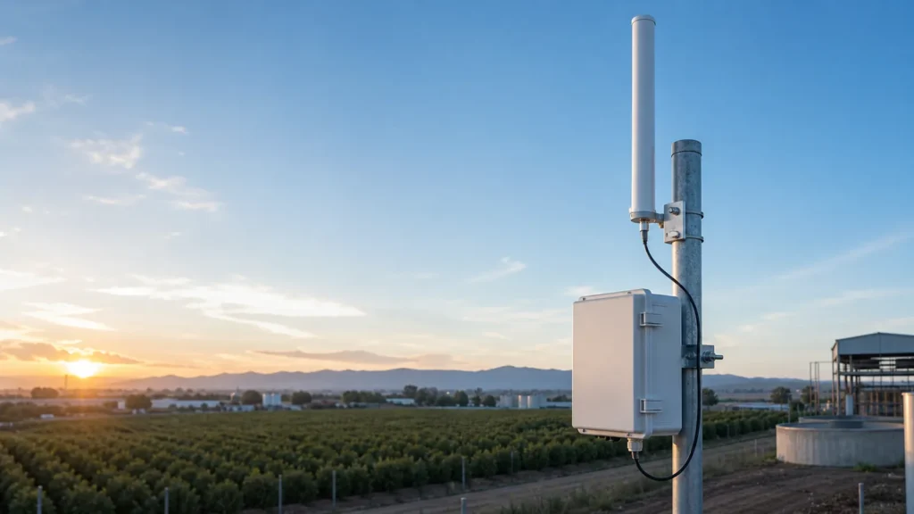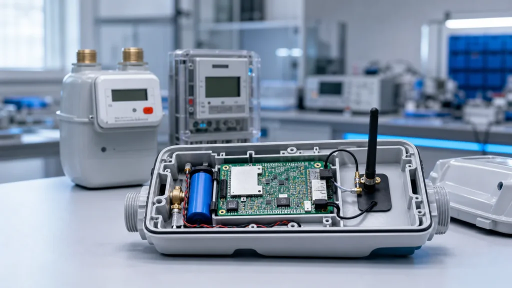

Choosing between a ceramic antenna and a PCB antenna is not a contest between two materials. Ceramic chip, PCB trace and FPC antennas can all fit inside the same wireless product, and none of them removes the antenna work — they only move it: into a component you buy and lay out, into copper you design and tune, or into a flexible part you place, cable and assemble.
Short answer: decide in this order — the regulatory band plan you must cover, the board and enclosure area you can actually reserve, and the certification path for the finished device. A ceramic chip antenna fits a tight, well-defined band. A PCB trace antenna fits reserved board edge area plus in-house RF tuning. An FPC antenna fits products where the enclosure offers a better antenna position than the PCB. The five steps below work through that decision.
One terminology correction first, because most comparison articles skip it. A PCB trace antenna is etched directly into the rigid product PCB. An FPC antenna is a separate printed radiator on a flexible film, normally connected to the radio with a coax cable or spring contacts. They are two different architectures, not two names for the same thing.

The three embedded antenna architectures
Ceramic chip antenna
A ceramic chip antenna is a discrete component mounted on the PCB. The ceramic has a high dielectric constant (a material property that slows the radio wave down and lets the same resonance fit in a smaller part), so the component itself is small. The installed antenna is still much bigger than the part: it depends on the specified ground region, the keep-out area, the feed line, the matching network and whatever sits nearby.
GL916R35 is a current example. Its page publishes 916.0 ±3 MHz, RHCP polarization and VSWR no greater than 2 within the stated bandwidth — a compact, well-defined single-band part.
PCB trace antenna
A PCB trace antenna is formed in the copper of the rigid board. There is no antenna component to buy, but the radiator and its keep-out area consume board edge space, and its behaviour is tied to the real stack-up, ground plane, feed, enclosure and nearby components.
A trace works well when the mechanical and RF teams reserve the antenna region early and the project can afford prototype tuning. A copied reference shape is a starting point, never a finished design: change the board outline, the layer stack or the ground plane and the resonance moves.
FPC antenna
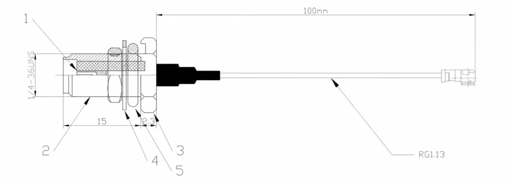
An FPC antenna puts the printed radiator on a flexible film, separate from the main board. A cable and connector let you mount it on a plastic surface inside the enclosure — away from shields, batteries and board noise. That freedom is the main reason to choose it.
GLFPC01 publishes 698–960 and 1710–2700 MHz coverage, vertical polarization, VSWR no greater than 2, a U.FL connector and a 70 × 20 × 2.5 mm form.
GL916R35 and GLFPC01 work in different bands with different design targets. Their datasheets illustrate two architectures; they are not a controlled head-to-head performance test.

Side-by-side comparison
| Factor | Ceramic chip | PCB trace | FPC |
|---|---|---|---|
| Radiator | Separate ceramic component | Copper on the main rigid PCB | Copper on a separate flexible film |
| Placement | Fixed to the main PCB | Fixed to the main PCB geometry | Can move within cable and enclosure limits |
| Board impact | Component land, feed, keep-out and ground requirements | Radiator and keep-out consume board area | Connector and feed on board; radiator uses enclosure area |
| Part and assembly | Discrete component plus matching parts | No separate radiator component | Radiator, cable/contacts and a placement step |
| Tuning sensitivity | Depends on supplier layout, ground and enclosure | Strongly tied to stack-up, ground and enclosure | Affected by mounting surface, cable routing and nearby material |
| Where the engineering effort goes | Following the reference layout and tuning the match | Designing and iterating the radiator geometry | Mechanical placement, cable routing and repeatability |
| Best fit | Tight, well-controlled single- or defined-band layout | Reserved board area plus in-house RF development | A better antenna position away from the main PCB |
No row declares a universal winner. A ceramic part can be tiny and still perform badly in the wrong layout. A trace can delete one BOM line and eat expensive board area. An FPC can improve placement and add cable, connector and assembly variation.
Step 1: Start from the band plan, not the antenna type
List every transmit and receive band the product must support, then check whether one radiator can cover them with margin. The regulatory band plan — not the substrate name — sets the bandwidth you have to hit.
| Use case | Frequencies the radiator must cover | Rule or specification |
|---|---|---|
| US unlicensed sub-GHz | 902–928 MHz (the same rule also covers 2400–2483.5 and 5725–5850 MHz) | 47 CFR §15.247; designated for ISM in ITU Region 2 with a 915 MHz centre frequency under Radio Regulations footnote 5.150 |
| European short-range devices | Sub-bands inside 863–876 MHz and 915–921 MHz, plus 433.05–434.79 MHz | ETSI EN 300 220-2, SRD 25–1000 MHz |
| Cellular 900 MHz | 880–915 MHz uplink and 925–960 MHz downlink, 45 MHz duplex spacing | 3GPP LTE Band 8, as listed in the LTE frequency band tables |
This is where a lot of projects go wrong. A part centred on 916 ±3 MHz is a good match for a US 902–928 MHz link, but “900 MHz cellular” means a radiator that stays matched from 880 to 960 MHz — about 8.7% relative bandwidth around 920 MHz. Same headline frequency, completely different bandwidth requirement.

So do not read the GL916R35 and GLFPC01 datasheets as proof that ceramic is always narrowband and FPC is always wideband. Bandwidth comes from the whole design — radiator, ground, match and enclosure — not from the substrate.
For GNSS receivers the usual ceramic form is a patch built around circular polarization and sky-facing placement. That is a separate selection job; see the GPS/GNSS ceramic patch antenna category.
Step 2: Size the antenna region, not the antenna
The component outline in a datasheet is the smallest number in the whole exercise. What you actually have to reserve is a region.
Start with a back-of-the-envelope check you can do before any layout:
λ (metres) ≈ 300 / f (MHz)
quarter wave ≈ λ / 4
At 915 MHz that gives λ ≈ 32.8 cm and a quarter wave of about 8.2 cm. At 2.45 GHz, λ ≈ 12.2 cm and a quarter wave of about 3.1 cm. Inside a dielectric the wave travels slower, so a printed radiator shrinks by roughly the square root of the effective dielectric constant — on FR4 (εr ≈ 4.4) a 2.45 GHz quarter wave lands near 1.5 cm instead of 3.1 cm. Treat these as engineering estimates for early feasibility, not measured dimensions; the real geometry comes out of simulation and prototype tuning.
That arithmetic explains the architecture choice better than any “which one is better” table. The lower the band, the more physical length a printed radiator needs, and the more attractive a high-dielectric ceramic part or a repositionable FPC becomes.
Then measure three separate spaces:
- Board area for the radiator, feed and keep-out.
- Three-dimensional clearance from batteries, shields, displays, motors and cables.
- Enclosure surface or volume for an FPC or external element.
And remember the part that datasheets state but layouts often ignore: for most small embedded antennas the PCB ground plane radiates too. Move the antenna from a long board edge to a short one, or shrink the ground, and both the resonance and the match change even though the antenna part number did not.
Step 3: Check the certification and connector rules before layout
This is the step most comparison articles leave out, and it can invalidate an architecture that looked fine electrically.
- The antenna is part of the authorisation. Under 47 CFR §15.203, an intentional radiator must be designed so that no antenna other than the one supplied by the responsible party can be used. A permanently attached antenna, or one using a unique coupling, satisfies this — but a standard antenna jack or electrical connector is prohibited.
- That is why embedded FPC antennas use miniature connectors. A U.FL-class interface is a practical way to keep the antenna non-user-replaceable while still shipping it as a cable assembly. Decide the connector and the compliance documentation together, not after testing.
- Ceramic and trace antennas are not exempt. They are simply permanently attached by construction, which is the easy path through this rule.
- If you integrate a certified radio module, the antenna is constrained by the module’s grant. FCC guidance in KDB 996369 puts the burden on the host integrator to follow the module instructions; swapping in a different antenna can require further assessment or a new authorisation.
Practical consequence: fix the antenna architecture before you freeze the enclosure and the compliance plan. A late switch from a trace to a cabled FPC is a mechanical change, a BOM change and a compliance-documentation change at the same time.
Step 4: Budget the engineering work honestly
Each architecture front-loads a different cost, and the invisible one is usually engineering time.
- Ceramic chip: low design risk if you follow the supplier’s ground, keep-out and matching guidance. You pay per unit, plus matching components. Expect at least one tuning round on the real board.
- PCB trace: no radiator component, so the recurring cost is board area. You pay in layout iterations, simulation and prototype rounds. Every stack-up or outline change reopens the tuning.
- FPC: moderate part cost, plus cable, connector and a placement step. The risk moves to repeatability — cable routing, bend radius and how consistently the film is fitted on the line. Cable length also costs a little signal, so keep runs short and specify the routing instead of leaving it to the operator.
Step 5: Validate in the finished product
All three architectures need final-device validation, in the production-intent enclosure, with the battery, display, shields and cables present.
A good VSWR alone proves very little. Measure what the link actually depends on: radiated efficiency, total radiated power, pattern and receiver sensitivity. For cellular and many connected products this is already formalised — CTIA’s over-the-air test plan defines radiated RF power and receiver performance methods for wireless devices, and it is a reasonable model for your own bench testing even when certification does not require it.

Quick decision guide
- Choose a ceramic chip antenna when the required band is well defined, space is tight, and the PCB can follow the specified ground plane and keep-out design.
- Choose a PCB trace antenna when you control the board and enclosure, can reserve enough edge area, and have the RF resources to tune the radiator as part of the product.
- Choose an FPC antenna when the enclosure offers a better antenna position than the main board, and assembly can control cable routing, connector mating and repeatable placement.
If those conditions are unclear, carry more than one architecture into the first prototype. Measurements in the real product should close the decision.
Common mistakes worth avoiding
- Comparing datasheet component sizes instead of the required antenna regions.
- Copying a reference trace layout onto a different stack-up or board outline.
- Treating a headline frequency as a band plan, then discovering the duplex gap later.
- Choosing a cabled FPC without checking the connector and authorisation rules.
- Signing off on VSWR measured on a bare board, then meeting the enclosure for the first time in the field.
Send the band, PCB and enclosure for an embedded antenna review
Prepared by the Rftech Technical Team from current product pages, embedded-antenna layout references and published regulatory documents (FCC 47 CFR Part 15, ETSI EN 300 220, ITU Radio Regulations, 3GPP band tables). Revised August 21, 2026; confirm current drawings, current rule versions and final-device measurements before layout release.
Ask our AI antenna assistant. Enter a keyword or question for a free answer based on this article, Global RF Tech content, and general antenna/RF knowledge.
Do not submit confidential or personal information. Privacy Policy