
Engineers asking what is a ceramic antenna usually want one answer: will this tiny part still work once it sits inside my enclosure?
Short answer. A ceramic antenna is a small radiating element built on a block of high-dielectric-constant ceramic. The ceramic shrinks the antenna electrically, so it resonates in a fraction of the space a wire or PCB trace needs. The chip is only part of the antenna: the PCB ground plane, the clearance around it and the enclosure decide whether it reaches its rated efficiency. Judge a candidate on ground-plane length, metal clearance and total efficiency, not on package size or peak gain.
Those three criteria (ground plane, clearance, and band coverage after integration) are what this article uses to decide whether a ceramic antenna fits a design. RFTECH’s GL916R35, a 916 ± 3 MHz ceramic part for LoRa / ISM 915 with VSWR ≤ 2.0, is the running example.
What makes a ceramic antenna different?
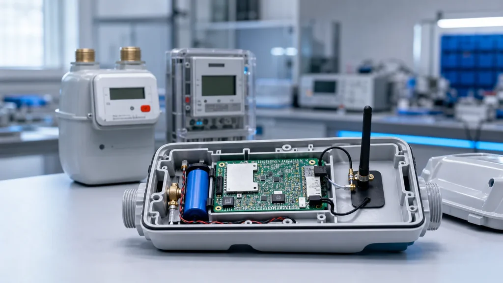
An external antenna radiates from an exposed structure. A ceramic antenna is mounted on the board and works inside a tightly constrained RF environment. It is an embedded part, not a visible one, which is what makes it attractive when a product needs:
- Compact dimensions
- A clean exterior with no protruding antenna
- Fewer exposed mechanical parts
- Tight integration into a sealed enclosure
The same integration is also the catch. Because the antenna shares space with the rest of the system, the PCB, battery, shield can, housing and nearby components all change how it tunes and radiates.
Two physical facts explain most of what follows:
- A high dielectric constant slows the wave inside the ceramic, so the resonant structure gets shorter by roughly the square root of that constant. That is the “shrinking” effect.
- Shrinking an antenna costs bandwidth and efficiency. For an electrically small antenna, size, bandwidth and efficiency are bounded together by the Wheeler–Chu limit, so no ceramic formulation delivers small, wideband and efficient at the same time.
Common ceramic antenna bands
Most ceramic chip antennas are tuned for one band, and those bands are set by radio regulation rather than by antenna fashion.
| Band | Frequency | Regulatory reference | Typical use |
|---|---|---|---|
| Sub-GHz ISM (US) | 902–928 MHz | FCC 47 CFR §15.247 | LoRa, ISM telemetry (e.g. GL916R35 at 916 MHz) |
| Sub-GHz SRD (EU) | 863–870 MHz | ETSI EN 300 220-2 | LoRa, metering, sensors |
| GNSS L1 | 1559–1610 MHz (GPS L1 at 1575.42 MHz) | ITU RNSS allocation | GPS / GNSS positioning (ceramic patch antenna) |
| BLE / Zigbee / Wi-Fi | 2400–2483.5 MHz | FCC 47 CFR §15.247 | Bluetooth, Zigbee, 2.4 GHz Wi-Fi |
| Wi-Fi 5 GHz | 5725–5850 MHz | FCC 47 CFR §15.247 | Dual-band Wi-Fi |
Three regulatory details are worth checking before you pick a part:
- In the US, the unlicensed bands used by these antennas are 902–928 MHz, 2400–2483.5 MHz and 5725–5850 MHz, defined in FCC 47 CFR §15.247.
- In Europe, the 863–870 MHz SRD band is limited to 25 mW e.r.p. with a duty cycle of 0.1% or polite spectrum access, and transmission is not allowed in the alarm sub-bands 868.6–868.7, 869.2–869.4 and 869.65–869.7 MHz, per ETSI EN 300 220-2. The practical consequence: you cannot buy back antenna loss with more airtime, so efficiency has to come from the design.
- GNSS parts live inside 1559–1610 MHz, allocated internationally to the radionavigation-satellite service, with GPS L1 transmitted at 1575.42 MHz ± 12 MHz (NTIA band compendium).
Because a single ceramic element is tuned to its band, multi-band products usually need either a multiband design or one ceramic antenna per radio.
How much ground plane does it actually need?

Most datasheets say “a ground plane is required” and stop there. The more useful observation is that published integration guidance clusters around a quarter wavelength of the operating band along the board’s long edge, and has almost nothing to do with the millimetre-scale package.
| Band | Free-space wavelength | λ/4 | Ground-plane guidance commonly seen |
|---|---|---|---|
| 868 MHz | 346 mm | 86 mm | 80 × 40 to 90 × 50 mm reference boards |
| 915 MHz | 328 mm | 82 mm | 80 × 40 to 90 × 50 mm reference boards |
| 1575 MHz | 190 mm | 48 mm | 50 to 70 mm square reference grounds |
| 2450 MHz | 122 mm | 31 mm | around 35 mm of solid ground minimum |
| 5500 MHz | 55 mm | 14 mm | rarely the limiting factor |
The λ/4 column is calculated from λ = c / f. Treat it as an engineering reference for early feasibility work, not as a measured specification.
That pattern flips the selection order. Check whether your longest board edge can approach λ/4 for the target band before you compare part numbers. A 30 mm board that has to work at 868 MHz is not a “which ceramic antenna” problem; the ground plane cannot support the rated efficiency, because the ground plane is what radiates. The ceramic part is the structure that excites it.
Two layout rules follow from the same physics:
- Place it mid-point on the long edge, not wherever space is left at the end of layout. That position gives the antenna ground on both sides.
- Keep the clearance area free of copper on all layers. For two-port ceramic loop antennas, the resonance is set by the path length around the PCB cutout, and published simulation work in Microwave Journal shows that adjusting a nominal 4.25 mm cutout by ±0.5 mm visibly shifts the resonant frequency. Half a millimetre of layout convenience is a tuning change.
Where ceramic antennas are commonly used
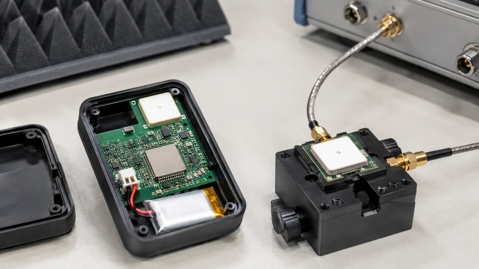
Ceramic antennas show up in IoT devices, smart sensors, compact asset trackers, consumer electronics, navigation terminals and embedded wireless modules. In nearly all of them the team is balancing RF performance against industrial design, battery size, connector elimination and assembly simplicity, so the antenna is judged as part of the whole device rather than as an isolated RF part.
Main benefits of a ceramic antenna
Small footprint
Dielectric loading lets the antenna fit layouts where a whip, panel or external mount would not physically go.
Better product integration
Because it lives inside the product, the device looks cleaner and avoids the mechanical failure modes of an external antenna.
Repeatable high-volume assembly
A surface-mount ceramic part supports consistent pick-and-place assembly across a product family with similar layouts, and simpler packaging.
A fit for modern IoT
As devices shrink and combine more radios, compact embedded antennas matter more, which is why ceramic parts come up so often in work like 2.4 GHz antennas for smart home IoT devices.
The tradeoffs engineers should understand
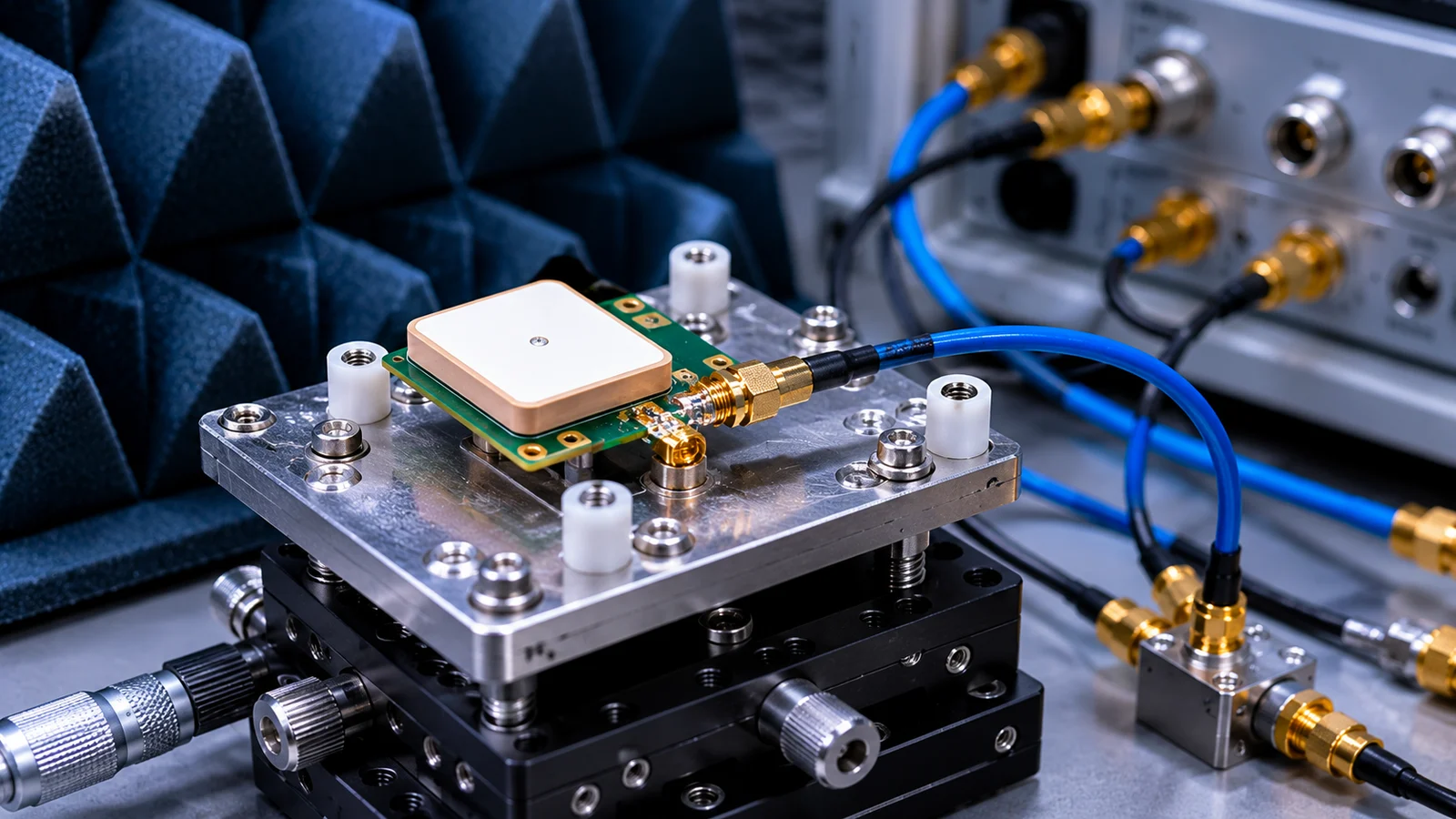
A ceramic antenna is not a miniature that fixes every RF problem. Its real tradeoff is sensitivity to the design around it.
The enclosure and nearby metal

Plastic is not neutral. A published TI measurement of a sub-GHz antenna mounted 1 mm from a plastic case shows the resonance moving from 868 MHz down to 862.875 MHz, with VSWR rising from 1.58:1 to 2.53:1 and roughly 18% of transmit power lost to reflection (TI application note SWRA726).
You can check that number yourself before any prototype exists:
Γ = (VSWR − 1) / (VSWR + 1)
reflected power = |Γ|²

VSWR 1.5 → 4% reflected
VSWR 2.0 → 11% reflected
VSWR 2.5 → 18% reflected
That is an engineering estimate from the mismatch alone, not a measured total loss, but it is enough to tell you whether a tuning shift matters. Metal is harsher than plastic. Commonly quoted clearance guidance puts under 10 mm between antenna and metal in the “severe loss” zone, 10 to 15 mm as workable, and over 15 mm as reduced coupling, which is why battery and shield-can positions belong in the antenna review, not in the mechanical review.
Placement
Moving the part a few millimetres changes the local layout around it, and therefore changes performance. Choose the antenna position first and route around it.
Ground plane
A chip antenna does not work in isolation. Ground plane size and shape usually decide whether the design hits its numbers, as the table above shows.
Bandwidth and efficiency
A small embedded antenna can be the right call, but only if the required band coverage and total efficiency are still acceptable after integration, measured on the assembled device rather than on a bench coupon.
Reading the datasheet: peak gain is not the number you want
Product pages usually lead with peak gain. It is the wrong first filter.
The number that predicts link performance is total efficiency. IEEE Std 145 defines realized (total) radiation efficiency as the radiation efficiency reduced by the impedance mismatch factor, so it already contains both the loss in the structure and the loss from a poor match. Peak gain describes one direction only, and an IoT device rarely holds still in that direction.
Two published figures for same-band 2.4 GHz ceramic parts make the point:
| Part size | Volume | Stated efficiency | Stated peak gain |
|---|---|---|---|
| 8.0 × 3.0 × 1.3 mm | 31.2 mm³ | 78% | 1.39 dBi |
| 2.0 × 1.2 × 0.55 mm | 1.32 mm³ | 62% | 1.88 dBi |
Two conclusions come straight out of the arithmetic:
- Volume buys very little efficiency. 23.6 times the volume returns 10·log(0.78 / 0.62) ≈ 1.0 dB. Fixing the ground plane or moving the antenna away from the battery usually returns more than that for free.
- The smaller, less efficient part quotes the higher peak gain. A less uniform pattern raises the peak while lowering the average, so ranking candidates by peak gain can select the worse antenna for a randomly oriented device.
Practical order of operations: ground plane, then placement and clearance, then enclosure spacing, then matching network, and only then a different part number.
When a ceramic antenna is a strong fit
It is a strong candidate when:
- The device must stay compact
- An external antenna would hurt the industrial design or usability
- The board’s long edge can get close to λ/4 for the target band
- The product will be tuned and validated as a complete system
- The operating band and environment are well understood
A single-band part like the GL916R35 916 MHz ceramic antenna is straightforward to evaluate once the device envelope, ground size and operating band are defined.
When a ceramic antenna may not be the best choice
It may not fit when:
- The enclosure varies a lot between product versions
- The device sits next to large metal parts with less than 10 mm of clearance
- The board is far shorter than λ/4 at the target band
- The required range is aggressive for the product size
- The team needs a drop-in answer with no tuning work
- A complex multi-band requirement leaves too little layout margin
In those cases a different integrated or external architecture is usually more forgiving.
Ceramic antennas in multi-radio products
As devices combine cellular, GNSS, Wi-Fi, BLE and proprietary links, the problem stops being one RF chain and becomes coexistence, isolation and enclosure compromise. Each radio still needs its own share of ground and clearance, and two ceramic antennas placed on the same short edge will couple. That is why related work like cellular and GNSS antenna integration matters: a compact antenna still has to work inside the whole radio system.
A practical evaluation checklist
- What is the exact operating band and bandwidth requirement, and which regulation applies?
- How long is the board’s ground plane compared with λ/4 at that band?
- How much clearance can the antenna get, on every layer?
- How far are the battery, shield can and metal parts from the antenna?
- Is the housing geometry stable across production versions?
- Will the team tune and validate total efficiency on the final assembled device?
If those answers are clear, a ceramic antenna can be an excellent compact solution. If they are not, the selection is not ready yet.
Where ceramic antennas make sense
A ceramic antenna is a compact, dielectric-loaded embedded option for products where space and clean packaging matter, and it performs when the ground plane, clearance and enclosure are handled deliberately. If you are weighing it against a board or flexible option, compare ceramic vs PCB antennas. The part is small; the RF discipline around it is not. For an embedded design, start from the product catalog or request a quote and tell us your frequency band, enclosure size and PCB constraints.
Frequently asked questions
What is a ceramic antenna used for?
Compact, embedded wireless devices such as IoT sensors, asset trackers, modules and consumer electronics, where there is no room for an external antenna. They are common on sub-GHz ISM and SRD bands (863–870 MHz, 902–928 MHz), GNSS L1 (1575.42 MHz) and 2.4 GHz BLE / Wi-Fi.
Why does ceramic make an antenna smaller?
Ceramic has a high dielectric constant. Loading the radiating element with that material slows the wave and reduces the resonant size by roughly the square root of the dielectric constant, so the antenna works at a given frequency in much less space than an air or PCB-trace design.
Do ceramic antennas need a ground plane, and how big?
Usually yes. Published integration guidance tends to land near a quarter wavelength on the board’s long edge: roughly 80 to 90 mm at 868 to 915 MHz, around 48 mm at GNSS L1, and around 31 to 35 mm at 2.4 GHz. Too small a ground plane is one of the most common reasons a ceramic antenna misses its rated efficiency.
Should I choose by peak gain or efficiency?
Efficiency. Total (realized) radiation efficiency already includes mismatch loss, while peak gain only describes the strongest direction. A smaller part can quote a higher peak gain and still perform worse in a randomly oriented device.
Is a ceramic antenna the same as a chip antenna?
The terms overlap in practice, since most surface-mount “chip antennas” are ceramic. “Ceramic antenna” also covers larger ceramic patch antennas such as GNSS patches, so a chip antenna is one common form of ceramic antenna, not the only one.
Can one ceramic antenna cover multiple bands?
A single ceramic element is normally tuned to one band. Multi-band or multi-radio products generally use a multiband design or a separate antenna per radio, and must plan for isolation between them. Confirm the part’s exact band against your radio before selecting.
Does a plastic case affect a ceramic antenna?
Yes. A plastic wall close to the antenna acts as extra dielectric loading and pulls the resonance down. A published measurement shows a sub-GHz antenna 1 mm from a plastic case shifting from 868 MHz to about 863 MHz, with VSWR degrading from 1.58:1 to 2.53:1. Tune with the housing fitted, not on a bare board.
Ask our AI antenna assistant. Enter a keyword or question for a free answer based on this article, Global RF Tech content, and general antenna/RF knowledge.
Do not submit confidential or personal information. Privacy Policy